For more than 50 years, designers of computer chips mainly used one tactic to boost performance: They shrank electronic components to pack more power onto each piece of silicon.
Then more than a decade ago, engineers at the chip maker Advanced Micro Devices began toying with a radical idea. Instead of designing one big microprocessor with vast numbers of tiny transistors, they conceived of creating one from smaller chips that would be packaged tightly together to work like one electronic brain.
The concept, sometimes called chiplets, caught on in a big way, with AMD, Apple, Amazon, Tesla, IBM and Intel introducing such products. Chiplets rapidly gained traction because smaller chips are cheaper to make, while bundles of them can top the performance of any single slice of silicon.
The strategy, based on advanced packaging technology, has since become an essential tool to enabling progress in semiconductors. And it represents one of the biggest shifts in years for an industry that drives innovations in fields like artificial intelligence, self-driving cars and military hardware.
“Packaging is where the action is going to be,” said Subramanian Iyer, a professor of electrical and computer engineering at the University of California, Los Angeles, who helped pioneer the chiplet concept. “It’s happening because there is actually no other way.”
The catch is that such packaging, like making chips themselves, is overwhelmingly dominated by companies in Asia. Although the United States accounts for around 12 percent of global semiconductor production, American companies provide just 3 percent of chip packaging, according to IPC, a trade association.
That issue has now landed chiplets in the middle of U.S. industrial policymaking. The CHIPS Act, a $52 billion subsidy package that passed last summer, was seen as President Biden’s move to reinvigorate domestic chip making by providing money to build more sophisticated factories called “fabs.” But part of it was also aimed at stoking advanced packaging factories in the United States to capture more of that essential process.
“As chips get smaller, the way you arrange the chips, which is packaging, is more and more important and we need it done in America,” Commerce Secretary Gina Raimondo, said in a speech at Georgetown University in February.
The Commerce Department is now accepting applications for manufacturing grants from the CHIPS Act, including for chip packaging factories. It is also allocating funding to a research program specifically on advanced packaging.
Some chip packaging companies are moving quickly for the funding. One is Integra Technologies in Wichita, Kan., which announced plans for a $1.8 billion expansion there but said that was contingent on receiving federal subsidies. Amkor Technology, an Arizona packaging service that has most of its operations in Asia, also said it was talking to customers and government officials about a U.S. production presence.
Packaging chips together isn’t a new concept and chiplets are just the latest iteration of that idea, using technological advances that help cram the chips closer together — either side by side or stacked on top of one another — along with faster electrical connections between them.
“What is unique about chiplets is the way they are connected electrically,” said Richard Otte, the chief executive of Promex Industries, a chip packaging service in Santa Clara, Calif.
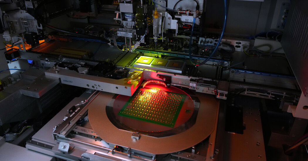
Chips can’t do anything without a way to connect them with other components, which means they need to be placed in some kind of package that can carry electrical signals. That process starts after factories complete the initial phase of manufacturing, which may create hundreds of chips on a silicon wafer. Once that wafer is sliced apart, individual chips are typically bonded to a key base layer called a substrate, which can conduct electrical signals.
That combination is then coated in protective plastic, forming a package that can be plugged into a circuit board that is essential for connecting to other components in a system.
These processes originally required lots of manual labor, leading Silicon Valley companies to shift packaging to lower-wage countries in Asia more than 50 years ago. Most chips are typically flown to packaging services in countries like Taiwan, Malaysia, South Korea and China.
Since then, packaging advances have gained importance because of the diminishing returns from Moore’s Law, the shorthand expression for chip miniaturization that for decades drove progress in Silicon Valley. It is named for Gordon Moore, a co-founder of Intel, whose 1965 paper described how rapidly companies had doubled the number of transistors on a typical chip, which improved performance at a lower cost.
But these days, smaller transistors are not necessarily cheaper, partly because building factories for leading-edge chips can cost $10 billion to $20 billion. Big, complex chips also are costly to design and tend to have more manufacturing defects, even as companies in fields like generative A.I. want more transistors than can currently be packed onto the biggest chips manufacturing machines allow.
“The natural response to that is putting more things in a package,” said Anirudh Devgan, chief executive of Cadence Design Systems, whose software is used to design conventional chips as well as chiplet-style products.
Synopsys, a rival, said it was tracking more than 140 customer projects based on packaging multiple chips together. As much as 80 percent of microprocessors will use chiplet-style designs by 2027, according to the market research firm Yole Group.
Today, companies typically design all the chiplets in a package along with their own connection technology. But industry groups are working on technical standards so companies can more easily assemble products from chiplets that come from different makers.
The new technology is mostly used now for extreme performance. Intel recently introduced a processor called Ponte Vecchio with 47 chiplets that will be used in a powerful supercomputer at Argonne National Laboratory, which is near Chicago.
In January, AMD disclosed plans for an unusual product, the MI300, that combines chiplets for standard calculations with others designed for computer graphics, along with a large pool of memory chips. That processor, intended to power another advanced supercomputer at Lawrence Livermore National Laboratory, has 146 billion transistors, compared with tens of billions for most advanced conventional chips.
Sam Naffziger, an AMD senior vice president, said it wasn’t a slam-dunk for the company to bet its chip business for server computers on chiplets. Packaging complexities were a major hurdle, he said, which were eventually overcome with help from an undisclosed partner.
But chiplets have paid off for AMD. The company has sold more than 12 million chips based on the idea since 2017, according to Mercury Research, and has become a major player in microprocessors that power the web.
Packaging services still need others to supply the substrates that chiplets require to connect to circuit boards and one another. One company driving the chiplet boom is Taiwan Semiconductor Manufacturing Company, which already makes chips for AMD and hundreds of others and offers an advanced silicon-based substrate called an interposer.
Intel has been developing similar technology, as well as enhancing less-expensive conventional plastic substrates in an approach favored by some such as the Silicon Valley start-up Eliyan. Intel has also been developing new packaging prototypes under a Pentagon program and hopes to win CHIPs Act support for a new pilot packaging plant.
But the United States has no major makers of those substrates, which are primarily produced in Asia and evolved from technologies used in manufacturing circuit boards. Many U.S. companies have also left that business, another worry that industry groups hope will spur federal funding to help board suppliers start making substrates.
In March, Mr. Biden issued a determination that advanced packaging and domestic circuit board production were essential for national security, and announced $50 million in Defense Production Act funding for American and Canadian companies in those fields.
Even with such subsidies, assembling all the elements required to reduce U.S. dependence on Asian companies “is a huge challenge,” said Andreas Olofsson, who ran a Defense Department research effort in the field before founding a packaging start-up called Zero ASIC. “You don’t have suppliers. You don’t have a work force. You don’t have equipment. You have to sort of start from scratch.”
Ana Swanson contributed reporting.